Proceedings · Session S-576 · filed September 26, 2026
Physical Sciences ResearchSession paper
X-ray imaging catches oxide coatings halving graphene fields
Photoemission microscopy maps fields in operating graphene devices, showing oxide coatings cut local fields by over 50% via p-type charge-transfer doping.
By Tom Whitfield3 min read533 words
Summary
- Metal-oxide coatings suppress local electric fields in operating graphene devices by more than 50%, measured directly by scanning photoemission microscopy.
- The mechanism is p-type charge-transfer doping: oxides remove electrons from graphene, flattening the voltage gradient; cross-checks against electrical measurements confirm the effect is purely electrostatic.
- Published as Umidakhon Rayimjonova et al 2026 Rep. Prog. Phys. 89 060502, from Uppsala University.
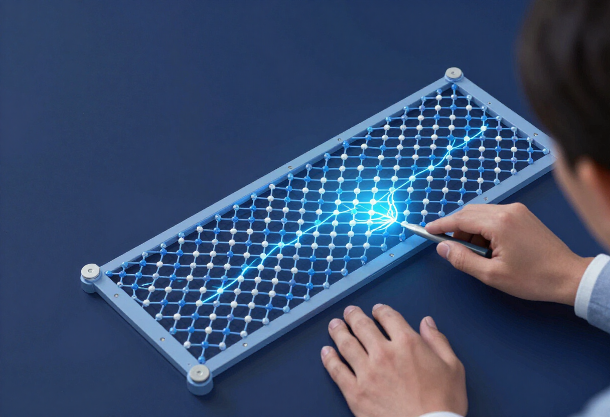
Researchers have directly mapped electric fields inside working graphene devices for the first time, and measured that ultrathin metal-oxide coatings suppress local fields by more than 50%. The result, published as Umidakhon Rayimjonova et al 2026 Rep. Prog. Phys. 89 060502, replaces a decade of inference from resistance data and simulation with spatially resolved measurement.
The team, working with Umidakhon Rayimjonova and M. Venkata Kamalakar of Uppsala University, used spatially resolved scanning photoemission microscopy (SPEM) built on X-ray photoelectron spectroscopy to map electrical potentials across graphene devices while current flowed through them. From these maps they reconstructed the electrical landscape: steep potential slopes mark strong electric fields, flat regions mark weak ones. Overlaying the maps onto device geometry shows exactly where oxide coatings alter that landscape.
The context matters for anyone building 2D-material devices. Aluminum oxide and titanium oxide layers are routinely deposited on graphene in devices ranging from transistors to spin valves, deliberately modifying electron flow. Engineers have known these coatings change device behavior. What they lacked was any direct observation of the electrostatics inside an operating device. Until now, understanding rested on theoretical models, numerical simulations and indirect electrical measurements.
The measured mechanism is p-type charge-transfer doping. The oxide pulls electrons out of the graphene, altering the local electrostatic environment and flattening the voltage gradient. Local electric fields weaken accordingly — by more than half, according to the published figures. That is a large margin for device operation, and it is now a directly measured number rather than a model output.
The methodological check is worth noting. By making a direct comparison between the SPEM maps and conventional electrical measurements on the same devices, the researchers confirmed the observed suppression stems solely from electrostatics and charge redistribution, not from other effects such as contact behavior or measurement artifacts. That cross-validation is what separates this work from earlier indirect estimates.
For R&D managers, the implications touch three decisions. First, characterization: SPEM on operating devices gives a new qualification tool for 2D-material process lines, capable of catching field non-uniformities that resistance measurements average out. Second, design: local tuning of electric fields via patterned oxide coatings acts as an additional design knob, allowing different regions of one graphene circuit to be tuned independently. Third, portfolio: the effect matters most where devices are most field-sensitive — spintronics, where local fields directly affect performance, and neuromorphic hardware, which requires precise control of local electrical properties to implement its switching behavior.
The usual caveats apply when weighing the claims. The figure of "more than 50%" field suppression comes from specific oxide materials at specific thicknesses in this study; the paper does not claim the number generalizes to every deposition process or coverage geometry. Graphene's appeal — atomically thin carbon with highly tunable conductivity for high-speed electronics, spintronic devices and neuromorphic components — remains the driver, but each coating and process combination will need its own mapping.
Still, the core advance stands on its own: direct visualization of charge distributions and electric fields inside operating 2D-material devices at high spatial resolution. Work of this kind points toward oxide patterning becoming a standard, characterizable design element in graphene device fabrication.
via iopscience.iop.org (Original)
Filed under
- graphene
- 2d-materials
- x-ray-imaging
- electric-fields
- oxide-coatings
More from Tom Whitfield
Show full bio
Senior reporter covering media and advertising at Hypothesis Wire.
92 articles
References
- Applied Voltage Switches Exciton Transport in 2D Perovskite-WS2 Device
- Femtosecond Spectroscopy Settles WSe₂ Exciton Debate
- In-situ XAS decodes activity-durability trade-off in MXene-supported Pt alloys
- Sliding water droplets corrode Teflon-coated copper, Max Planck team finds
- Fraunhofer IFAM Opens Electrolysis Prototype Centre